
9 Facts Design Engineers Need to Know About Photo Etching
For design engineers, creating a new metal part design involves investing time in research, collaboration, and determining which materials and manufacturing processes are suitable. What further complicates this process is project deadlines and budgetary constraints.
When exhibiting at contract manufacturing shows, we meet many design engineers who are not familiar with photo etching. This lack of knowledge about the chemical etching process is understandable as there are only about 100 photo etching companies in the United States and a few hundred worldwide. Compare that with other metal fabrication technologies for thin metal components such as wire EDM, laser/plasma/ water jet cutting, stamping, electroforming, and CNC punching where the numbers are into the thousands
Photo etching, which uses chemical etchants to wash away the unwanted metal sections that are not part of the design, is an alternative to traditional machining methods for thin metal pieces.
You may be confused by the different terms used to describe photo etching: photochemical machining (PCM), chemical etching, metal etching, photo chemical milling, photo chemical etching or chemical milling. All of these names are accurate labels to describe the manufacturing process.
It is noteworthy to point out that the term chemical milling is synonymous with chemical etching in that both are chemical machining processes, but in some instances use a slightly different method.
Chemical milling also refers to machining on three-dimensional parts. However, a different masking material other than photoresist is used to protect the part's surface from the chemical etchant. It is most frequently used on aerospace parts to reduce weight without compromising strength and function.
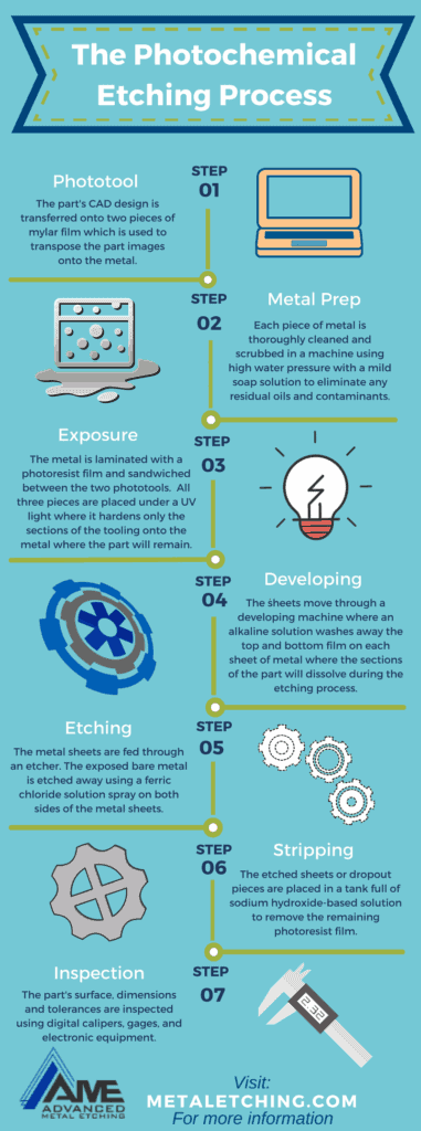
Before you understand how photo chemical etching can benefit your design, it is necessary to explain the photo chemical etching process.
Below is an infographic detailing the steps:
The benefits of photo etching include reduced costs, shorter lead times, flexible tooling, unaltered metal properties, and burr-free components with low tolerances. The process is capable of etching prototypes to large production runs with a variety of metals.
The following nine facts about photo chemical etching will help design engineers decide if the chemical etching process is suitable for his/her next project.
1. Capabilities
How to determine if PCM is right for your design application? Let's take a look at the technical aspects of the machining process.
Standard metal etching machines can etch through metal within a range of 0.0005 to 0.080 in (0.013 to 2.032 mm).
There are over 50 types of metals that are favorable for the etching process. Some of the most popular are cold rolled steel, alloy 42, beryllium copper, brass, nickel silver, nickel, Kovar, copper, and phosphorus bronze.
Exotic metals such as aluminum, titanium, and Inconel are also available in some etching houses to meet the demand for lighter, stronger and heat resistant metal parts found in automotive and aerospace systems.
Standard metal sheet sizes run from 12' x 12", 12" x 18", 12" x 24" with some as large as 24" x 30". The goal is to optimize the chemical etching process by fitting as many parts on a sheet as possible.
The tooling engineer creates a photo tool from a CAD design of the part that is compatible with the design engineer's geometric dimensional tolerancing parameters.
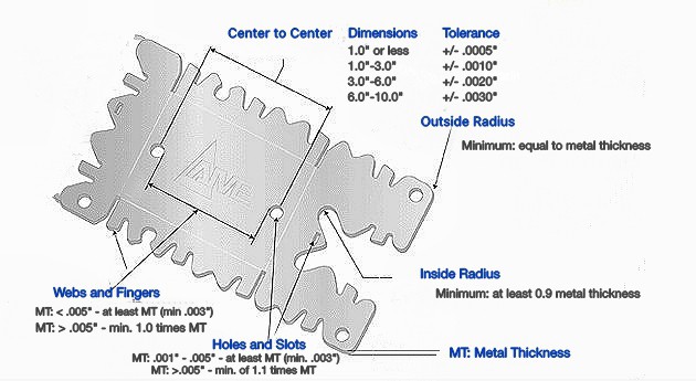
The following diagram of a thin metal part showcases the minimum and maximum dimensions for special features such as holes, slots, fingers, radii, and center to center tolerances.
Source: Advanced Metal Etching
As you can see from this diagram, depending on the metal thickness, there are limitations to the precision and size of small holes, slots, radii, and tolerances.
All machining methods will have similar restrictions, but, photo etching is the most cost-effective and precise when it comes to numerous intricate features as you will learn later in the article.
Another useful photo etching capability is half-etching. These markings provide score lines for the secondary forming operation often needed for parts such as EMI and RFI shielding. Other uses of half-etching are logos (see the AME on the diagram above) and numbers or other identifying marks.
2. Flexible Tooling
What happens if you need to make revisions to an existing prototype design? How much is it going to cost to make tooling changes?
The good news is that photo etching tooling is very cost-effective because of its flexibility. What does that mean?
Well, to put it in perspective, let's compare the tooling costs and time to the traditional mechanical tooling that you see in stamping or CNC punching.
Those manufacturing methods require "hard' metal tooling which is made out of dies. These dies can take weeks to make and are expensive.
The cost can range anywhere from $1,000 to several thousand dollars depending on the part's design. So, any modifications would be costly.
On the contrary, photochemical machining tooling is digital. With the use of CAD software, photo tools can be created within a day, which makes expedited shipping possible. The original tooling process which includes labor and imaging costs around $300.
But, if you need to revise the part, subsequent tooling will cost around $180. PCM manufacturers store tooling for life, which makes future production runs cost-effective and quick.
Time is money, and quick and flexible tooling is one of the advantages of the metal etching process that will save you both.
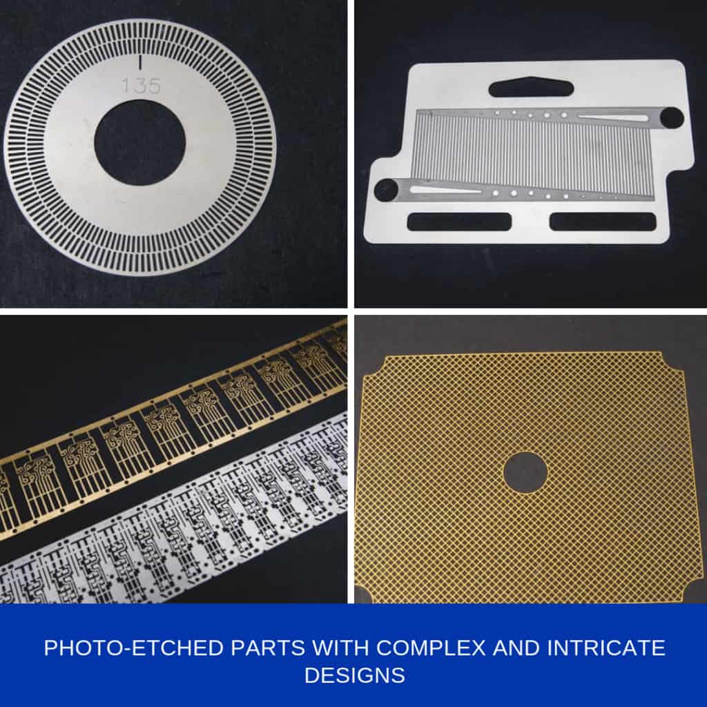
3. Intricate and Complex Designs
While photochemical machining is capable of etching any design whether it is as simple as washers, pins, contacts, or shielding components, it excels in the manufacturing of complex and intricate designs such as encoder disks, fuel cell plates, lead-frames, filters, and screens. Let's explore why it is a better alternative than laser cutting, wire EDM, stamping, etc.
During the photo etching process, the machines spray a chemical etchant evenly onto the top and bottom of the sheet. The metal surface of the exposed sections is etched away in the same uniform manner as ocean waves on sand. This even acid "erosion" creates a smooth surface while etching all the holes, slots, and other features at the same time while maintaining low tolerances.
Laser cutting and wire EDM processes take longer to manufacture because they are not cut simultaneously.
The stamping process requires progressive tooling which means more than one strike is necessary to get the needed features, thus requiring more than one die. Too many features = higher tooling costs and added stress on the metal. When it comes to complex designs, those methods don't compare.
If larger production volumes are required, photo etching will save time and money.
4. Cost-Effective
There are many reasons why photochemical machining proves to be one of the most cost-effective solutions for manufactured thin metal parts.
- Flexible digital tooling - Because digital tooling is easily modifiable, revisions are inexpensive making it an ideal process for prototypes. Also, if you have several prototypes with the same material and thickness, they can be processed on the same sheet of metal. This process is called compound tooling and can also save time.
- Lead time- Photo chemical etching companies can ship parts out within days to a week. Quickly processed tooling and in-stock metals make this possible, allowing you to get your products to your customer faster.
- Repeatability with Complex Features- Let's say you need 2,000 pieces of a part that is .60" (15.24 mm) in length and .11" (2.79mm) in diameter with many features, such as a stent for the medical industry. Using CAD software, the tooling engineer will design the pattern to fit as many parts as possible on the sheet. The machining operator will calibrate the speed, and the pieces will simultaneously etch making it more cost-effective than laser cutting, wire EDM and stamping which processes piece by piece.
5. Burr-Free With Low Tolerances
Many industries require parts to be free of burrs with even surfaces. In many electronic components such as contacts, connectors, and lead frames, clean surfaces and edges are necessary for parts to retain their conductive properties. Any imperfection can affect functionality. Moreover, clean parts are essential before plating so the material can adhere adequately to the metal.
Likewise, the burr-free chemical machining process is ideal for medical devices such as implants and surgical blades, which understandably require smooth surfaces and edges with low tolerances. Imperfections such as those can make a difference, literally, between life or death.
You will not find burrs on parts that are photo-etched.
In fact, except for electroforming, all other machining processes have some burr or mechanical stress.
Laser cutting, water jet cutting, and wire EDM machining can generate micro burrs, while stamping emits partial burring and stress on thinner metals.
Hard tooling, gases, or electrical currents are not present and will not cause interference with the part's function.
6. Metal Properties Remain Unaltered
When deciding which manufacturing process will be best for your design, there may be concerns about the impact of stress that hard tooling can impact on the metal. If the goal is low tolerances and conductivity, then any type of deformation can alter the part's function.
As electronics become smaller and lighter, so do their components.
Lead-frames are an excellent example of a thinner part with finer pitches, low tolerances, and more intricate designs.
Typically, they consist of copper or nickel because of their high thermal and electrical conductivity.
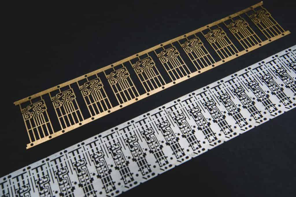
Photo etching copper and nickel lead-frames will ensure that the thermal and conductivity properties will remain intact. The chemical etching process doesn't change the metal hardness, grain structure, and flexibility.
Whereas, the laser cutting process emits heat and gas, which can cause thermal deformation, micro burrs or "whiskering".
The wire EDM process also creates heat in the form of electrical currents.
And, stamping with its force, can compromise the structure of very thin metals with complex designs.
7. Prototype To Large Volume Production
If you are starting to plan for the manufacturing phase and are seeking a metal fabricator, photo etching is an excellent choice for both prototyping and larger production runs.
As mention previously, compound tooling makes prototyping cost-effective. And even better, if the design needs tweaking, then it is easy to change.
When the right design is finalized, the photochemical etching process can scale part volume into higher quantities.
8. Technical Assistance
Tooling engineers can assist with metal selection and explain etching techniques.
Because experienced tooling engineers work with many different parts and metals, they can suggest design modifications to retain dimensional tolerances.
For example, to make parts more manageable for handling and shipping, the parts can remain in sheets.
If so, the tooling engineer would recommend either recessed or protruding tabs on each piece depending on the part's intended function.
9. Fast Turnaround
Because of its digital tooling and ability to etch many parts simultaneously, photo etching is a speedier metal fabrication process.
Lead times are typically within five to ten days, whereas stamping can take six to eight weeks.
If an order is "hot," then most prototypes or small batches can be manufactured and shipped the same day depending on the part and metal inventory.
It is advantageous to seek a photo etching company that has processes in place for expedited orders.
Bottom line: Photo etching is a viable manufacturing option to consider for your next design. With its speed, tooling flexibility, clean burr-free surfaces, low tolerances, and cost-effectiveness with intricate designs, photochemical machining is an excellent alternative to traditional machining methods.
Related Posts:
5 Ways to Lower Photo Etching Costs
5 Reasons Why Chemical Etching is Ideal for Electronic Components